
Our Applications
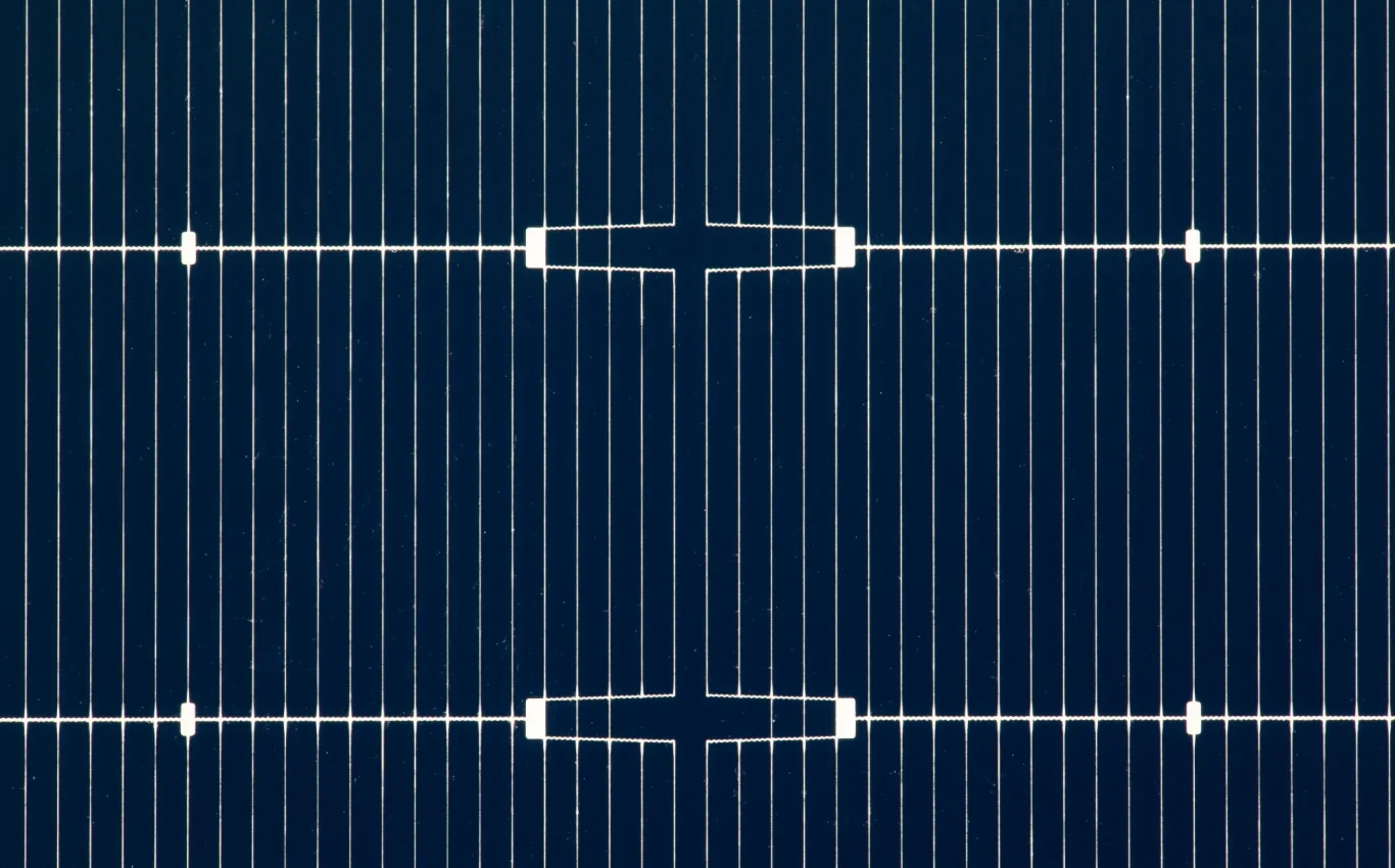
Solar Cell Metallization
We develop pastes for various printing methods applied on both conventional and next-generation solar cells. Our formulations enable significant savings without compromising conductivity or efficiency.
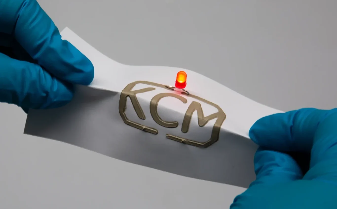
Flexible Printed Electronics & Sensors
Our technology enables flexible electronics with fewer conductive particles. This reduce material costs while improving mechanical flexibility and long-term durability.
Electrical Conductive Adhesives
We engineer electrically conductive adhesives that maintain high conductivity while reducing conductive filler content by lowering the amount of material needed to establish an effective conductive network.
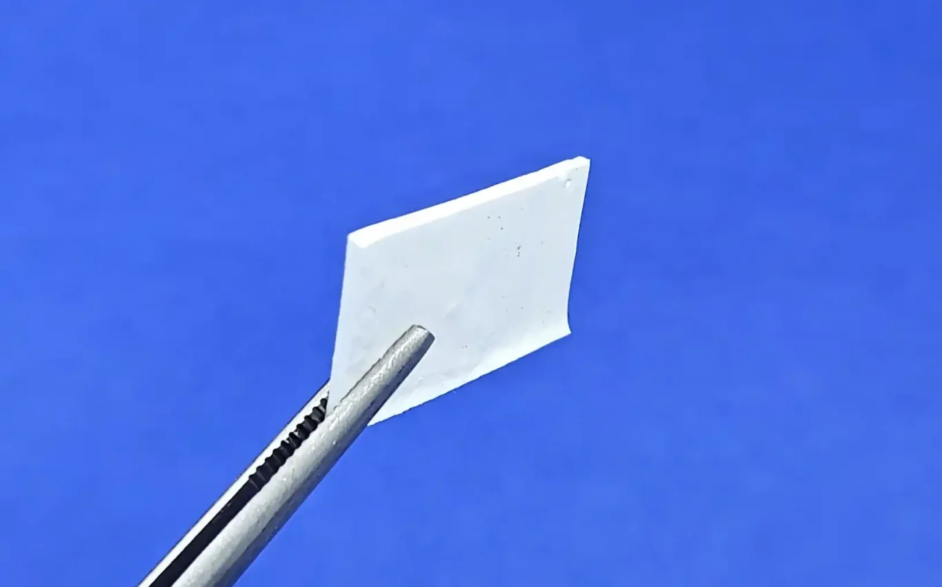
Thermally Conductive Pastes
Our technology enable the production of cost-efficient, thermally conductive materials with exceptional performance. Ideal for heat management in batteries and computer technology.
Compatibility with Standard Printing Technologies
To enable integration into existing production lines, the pastes must be designed for compatibility with industrial printing methods and established processes.
This includes the following process methods:
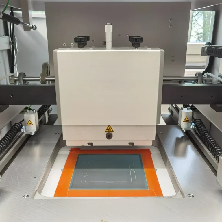
Screen printing is one of the most cost-effective printing techniques. It is the industry standard for many electronics applications and ideal for high-throughput manufacturing.
Dispensing features airtight fluid management and supports fast-curing, low-temperature formulations. Perfect for precise, automated application.
Stencil printing is a highly accurate method for applying paste to printed circuit boards. It ensures consistent layer thickness and precise pattern definition.
Case Study: Fine Line Printing for Solar Cells
The Challenge
Silver is one of the biggest cost drivers in solar cell production, above all in front-side metallization. Manufacturers need ways to print narrower contact lines with less silver, without losing conductivity or throughput.
Our Approach
Together with industrial partners, we developed high-performance pastes for fine-line metallization. They reduce silver consumption and are designed for industrial-scale production. We tested the technology on two cell types and with two printing methods, screen printing and dispensing:
- High-temperature cells: PERC and TOPCon
- Low-temperature cells: Heterojunction (HJT) and perovskite
Results
Our pastes combine fine lines with industrial throughput:
- Printing speeds above 500 mm/s
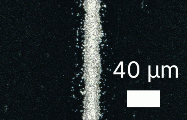
- Feature sizes down to 16 µm
- Up to 19 % less paste laydown
- Cell efficiencies of 23.53 % on PERC
High-temperature paste for screen printing
Low-temperature paste for dispense printing
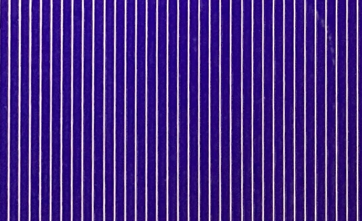
Dispensed onto the wafer, our paste produces highly uniform fingers:
- Line width: 35 ± 1 µm
- Aspect ratio: 0.48 ± 0.03
- Line resistivity: 31 ± 6 µΩ·cm (≈ 3 MS/m)
The benefit for manufacturers
Our pastes cut silver and paste consumption per cell while printing finer lines at industrial speeds, for both high- and low-temperature cell architectures. Manufacturers lower their costs, raise cell efficiency and make their production more sustainable.