
Next-generation conductive pastes for printed electronics
We develop high-performance formulations for printed electronics that combine superior conductivity with reduced use of precious metals - enabling more efficient, scalable, and cost-effective manufacturing.
Our project originates at the Karlsruhe Institute of Technology (KIT) and is supported by the Helmholtz Society’s spin-off program. We combine deep scientific expertise with a clear focus on industrial impact.
Industries are Increasingly Constrained by Costs
+475%
Silver Price
Adjusted for inflation, silver prices have increased significantly over the last 20 years.
80%
Material Costs
Precious metals such as silver account for a large portion of the cost of printed electronics pastes.
30%
Silver Costs in PV
In solar cell manufacturing, silver represents one of the largest material cost contributors.
A New Physical Concept
At KCM, we combine scientific innovation with industrial relevance. Our conductive pastes are built on a novel physical principle that enables superior performance while reducing material costs and environmental impact. The result: A technology platform that is not only powerful, but also practical, ready to scale, easy to integrate, and adaptable across applications.
Cost-Efficient
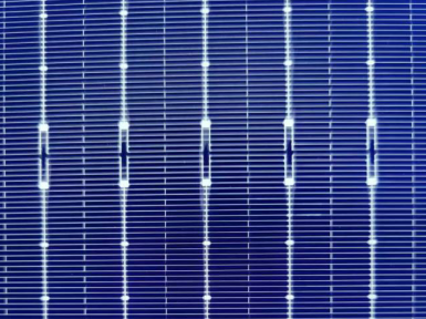
Thanks to our novel concept, we significantly reduce the use of precious metals like silver. This lowers material costs without compromising electrical or mechanical performance. Ideal for cost-efficient solar cells.
Exceptional Conductivity
Thanks to our innovative technology, our formulations achieve significantly higher conductivity than traditional formulation methods. As a result, they enable more efficient current transport and are well-suited for high-performance applications.

Process-Compatible
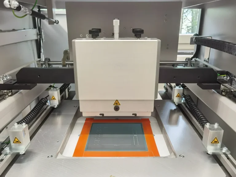
Our formulations are compatible with standard printing technologies such as screen printing, dispensing, and stencil printing. This simplifies integration into existing production lines.
Scalable
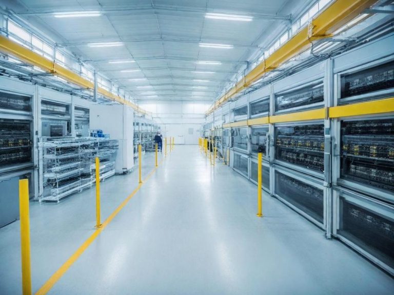
The materials we develop are designed for industrial-scale production and support high-throughput manufacturing. They can be manufactured using standard process routes and rely exclusively on non-hazardous components. This ensures a safe, cost-efficient, and sustainable implementation.
Universally Applicable
Our technology is material-independent which makes our approach adaptable to a wide range of formulations and application areas, from solar to flexible electronics.

Ready to Rethink Printed Electronics?

We’re currently looking for partners to test our prototypes, co-develop tailored solutions, and scale-up production.

Explore how KCM can help you reduce costs, save precious materials, and boost your performance.
Ready to rethink conductive pastes?
Electrical & thermal conductivity
Maximize conductivty
High conductivity by new formulation method. Ready for high-performance applications
Compatibility with Standard Printing Technologies
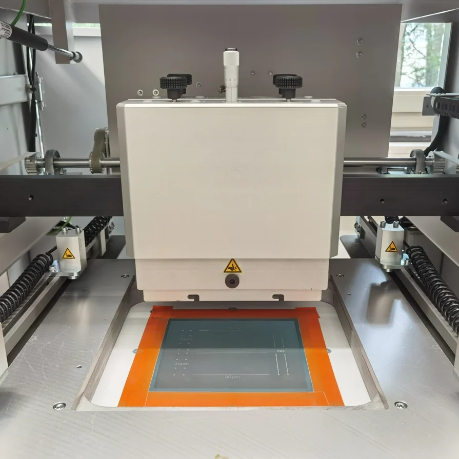
To enable integration into existing production lines, the pastes must be designed for compatibility with industrial printing methods and established processes.
This includes the following process methods:
Screen printing is one of the most cost-effective printing techniques. It is the industry standard for many electronics applications and ideal for high-throughput manufacturing.
Dispensing features airtight fluid management and supports fast-curing, low-temperature formulations. Perfect for precise, automated application.
Stencil printing is a highly accurate method for applying paste to printed circuit boards. It ensures consistent layer thickness and precise pattern definition.